Custom Fabrication

High-Security, High-Performance, Low-Volume Fabrication

NeutrinoX operates two highly specialized, Swiss and EU based semiconductor fabrication environments designed for programs that demand full supply chain trust, precision process control, and long-term support. Our vertically integrated approach allows us to support everything from process development to wafer delivery with full in-house design and test capability.

Our Office
Our Office
Our Office

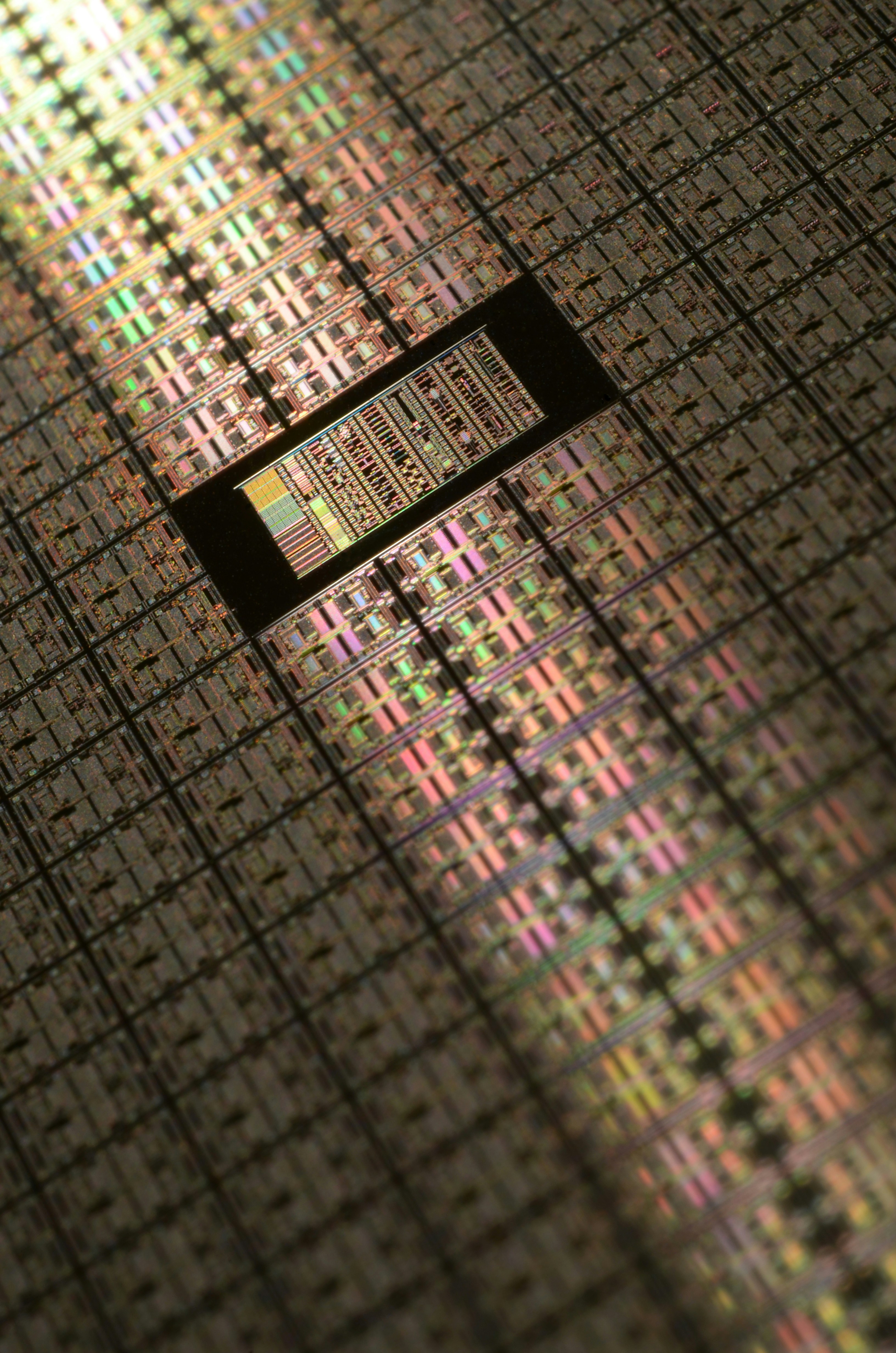
FD-SOI CMOS Fabrication (22nm Node)

Secure Silicon for Specialized Systems

Our proprietary 22nm Fully Depleted Silicon-On-Insulator (FD-SOI) CMOS platform is optimized for high-performance, low-power applications in the most sensitive environments.

/0

1

22nm FD-SOI node

ideal for RF/digital mixed-signal, low-noise, and radiation-hardened designs

/0

1

22nm FD-SOI node

ideal for RF/digital mixed-signal, low-noise, and radiation-hardened designs

/0

1

22nm FD-SOI node

ideal for RF/digital mixed-signal, low-noise, and radiation-hardened designs

/0

2

Low-volume production

supported (dozens to hundreds of wafers/year)

/0

2

Low-volume production

supported (dozens to hundreds of wafers/year)

/0

2

Low-volume production

supported (dozens to hundreds of wafers/year)

/0

3

ITAR-compliant

secure, air-gapped cleanroom environment

/0

3

ITAR-compliant

secure, air-gapped cleanroom environment

/0

3

ITAR-compliant

secure, air-gapped cleanroom environment

/0

4

Full-stack enablement

PDK, device modeling, design support available

/0

4

Full-stack enablement

PDK, device modeling, design support available

/0

4

Full-stack enablement

PDK, device modeling, design support available

/0

5

Trusted for use

Used in aerospace, defense, and secure comms SoCs

/0

5

Trusted for use

Used in aerospace, defense, and secure comms SoCs

/0

5

Trusted for use

Used in aerospace, defense, and secure comms SoCs

III-V InP Fabrication Lab

Indium Phosphide for High-Frequency RF & Photonics

Our III-V lab is dedicated to the production and prototyping of InP-based devices, delivering high-performance semiconductors for RF, millimeter-wave, and optoelectronic systems.

Applications:

  • Microwave & mmWave Power Amplifiers

  • InP-Based Mixers, Oscillators, and LNAs

  • Photonic Transceivers and DWDM Components

  • Scientific Imaging and Spectroscopy

/0

1

Specialized in InP-based HBTs, HEMTs, and optoelectronic devices

/0

1

Specialized in InP-based HBTs, HEMTs, and optoelectronic devices

/0

1

Specialized in InP-based HBTs, HEMTs, and optoelectronic devices

/0

2

Capable of custom process development for both active and passive device layers

/0

2

Capable of custom process development for both active and passive device layers

/0

2

Capable of custom process development for both active and passive device layers

/0

3

Processes tailored for high-frequency, high-linearity RFICs and photonic ICs

/0

3

Processes tailored for high-frequency, high-linearity RFICs and photonic ICs

/0

3

Processes tailored for high-frequency, high-linearity RFICs and photonic ICs

/0

4

Supports low- to medium-volume production for strategic defense, telecom, and scientific applications

/0

4

Supports low- to medium-volume production for strategic defense, telecom, and scientific applications

/0

4

Supports low- to medium-volume production for strategic defense, telecom, and scientific applications

/0

5

Internal packaging and test services available for turnkey module integration

/0

5

Internal packaging and test services available for turnkey module integration

/0

5

Internal packaging and test services available for turnkey module integration